|
高温超伝導体YBa2Cu3O7-xにおける人工ピンの導入法として,YBa2Cu3O7-δ と2次物質との多層膜を作製する方法を用いて,高磁場中での臨界電流密度Jcの改善やそのメカニズムとなる磁束ピンニング特性の解析を行っている.2次物質としては,Y2O3やCuサイトの一部を3d遷移金属元素であるZnで置換することを目的としたZnOを使用している(Figure 1). |
| 重イオン照射を利用したYBa2Cu3O7薄膜への照射欠陥導入 |
|
重イオン照射を用いることで,高温超伝導体に素性が明らかでバラエティな照射欠陥を人工ピンとして制御・導入することができる(Figure 2).ここでは,電子的阻止能を制御することで,超伝導体試料内に1次元ピンとなる柱状の欠陥から,3次元ピンである球状の欠陥へ系統的に変化させ,その磁束ピンニング特性について調べている. |
Fabrication of YBa2Cu3O7-x multilayered films with nanoparticles : The multilayered films were made with pulsed laser deposition on SrTiO3 substrates. The nano-particles of Y2O3 or ZnO on YBa2Cu3O7-δ layers were observed when several laser pulses for ZnO target ablation were chosen (Figure 1).
Introduction of irradiation defects into YBa2Cu3O7-x films : We investigate the influence of the columnar defects produced by the heavy-ion irradiation, which are long-correlated defects with its just features, on the pinning properties of YBa2Cu3O7-x films(Figure 2). It is found that the value of z, which is one of the pinning parameters, showed the peak behavior around the magnetic filed related with the fluence of the irradiation.
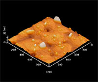
Figure 1 ZnO nano-dots grown on YBa2Cu3O7-x by 2 pulses. |
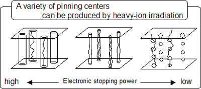
Figure 2 Magnetic field dependence of the dynamic critical exponent z |
|